- 유관기관
- 전북대 산학협력단
- 서울대 반도체공동연구소
- 경북대 반도체공정교육센터
- 연구기관
- ETRI(한국전자동신연구원)
- 한국전기연구원
- 한국광기술원
- 나노종합기술원
- 한국나노기술원
- 관련정부부처 및 재단
- 교육부
- 과학기술정보통신부
- 정보통신산업진흥원
- 산업통상자원부
- 한국연구재단
- 한국산업기술평가관리원
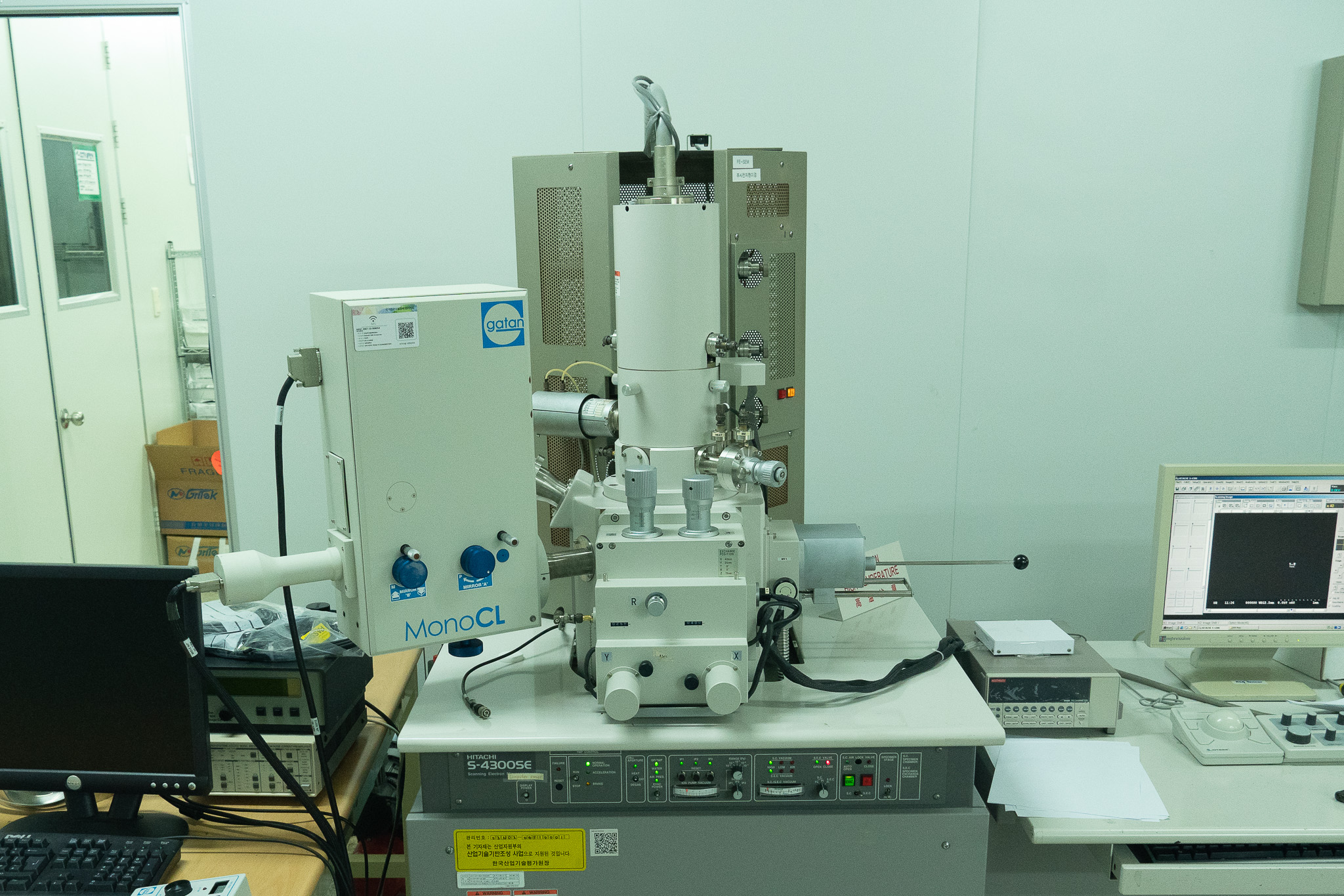
장비 > FE-SEM
| FE-SEM | |||||
|---|---|---|---|---|---|
| 작성자 | jnsinc | 등록일 | 21-01-20 15:44 | 조회 | 517 |
| 제작사 | Hitachi | 모델명 | S-4300 SE | 도입연도 | 2004-01 |
| 용도 | 반도체소자를 포함한 여러 물질의 표면형태 분석과 부속장치를 이용한 Cathodoluminescence 측정 및 Lithography 공정 | ||||
|
- 1.5 (at accelerating voltage of 15kV Working distance of 5mm) - 5.0 (at accelerating voltage of 1kV Working distance of 5mm) ? Magnification : -20x to 500000x ? Electron Optics - Electron gun : Cold-cathode field emission electron gun (ZrO/W) - Emission extracting voltage(Vext) : 0 to 6.5 kV - Schottky emission source Accelerating voltage (Vacc) : 0.5 to 30kV (in increment of 0.1kV/step) - Lens system : Electromagnetic lens reduction system - Objective lens aperture : Movable self-cleaning type thin aperture ? Specimen Size : 120 ~ 160 mm dia |
|||||
| 첨부파일 |
SEM.jpg |
||||
;)